home
download
documentation
mailing lists
wiki
IRC
forums
daily builds
feature requests
bug reports
patches
Hardware Components Overview of the iRiver H1xx
- Datasheets and chip images
- Motorola Integrated Microprocessor SCF5249
- Fairchild LVX245 - Low Voltage Octal Bidirectional Transceiver
- K4S561632E-TL75 - 4M x 16bit x 4Banks Synchronous DRAM LVTTL (256Mbit/32MB)
- 39VF160 - 2 MB Flash ROM
- UDA1380TT - Philips Stereo audio coder-decoder
- TXD - RXD connectors
- TLV08341 - 3-Volt 8-Bit Analog-to-Digital Converters With Serial Control (Rev. B)
- TEA5767 - Low-power FM stereo radio for handheld applications.
- ISSI 401-3G - 1kbit EEPROM
- ISSI IS25C02 - 2kbit EEPROM
- MEC-AL4A2 - 11.2896MHz oscillator
- LVCH16245A - 16-Bit Bus Transceiver With 3-State Outputs
- LW052A - Dual 4-Channel Analog Multiplexer/Demultiplexer
- AZU 3AW ZD5L (the 5 could be an S or even an 8)
- Micropower Synchronous Buck-Boost DC/DC Converter
- The LCD module
- The Buttons
- Remote Control
Datasheets and chip images
Motorola Integrated Microprocessor SCF5249
| |
This is the CPU at the heart of the player. For more information, go to ColdFire.
Fairchild LVX245 - Low Voltage Octal Bidirectional Transceiver
| |
Probably used for buffering the data bus, we may find more of these on the back, underneath the ATA interface daughterboard.
Info: http://www.fairchildsemi.com/pf/74/74LVX245.html
Datasheet: http://www.fairchildsemi.com/ds/74/74LVX245.pdf
K4S561632E-TL75 - 4M x 16bit x 4Banks Synchronous DRAM LVTTL (256Mbit/32MB)
| |
39VF160 - 2 MB Flash ROM
16 Mbit (x16) Multi-Purpose Flash (SST39VF160)
| |
Info: http://www.sst.com/products.xhtml/parallel_flash/39/x16/SST39VF160
Datasheet: http://www.sst.com/downloads/datasheet/S71145.pdf rockbox
Driver Example: http://www.sst.com/downloads/software_driver/SST39VF160.txt
UDA1380TT - Philips Stereo audio coder-decoder
This chip can NOT decode MP3 (or any other codec format) - codec decoding is performed on the ColdFire CPU.The chip contains stereo digital->analog & analog->digital converters. The UDA1380 has sound processing features in playback mode, de-emphasis, volume, mute, bass boost and treble which can be controlled by the L3-bus or I²C-bus interface.
| |
Info: http://www.semiconductors.philips.com/pip/UDA1380TT_N1.html
Datasheet: http://www.semiconductors.philips.com/acrobat/datasheets/UDA1380_4.pdf
LucaBurelli: By checking the block diagram and the information on the pages above, it appears that the H1xx could be used for radio recording too! The "external input" on this IC (which is probably commuted by the analog muxes between radio and the line in jack) is connected to both the DAC and the line out via an amplifier. So it should work... anyone double check this idea, please?
DaveHooper: From analysis of the firmware, it seems there is an "recording source" option of "TUNER" (which is unavailable from the user interface). Also others have commented that the record from radio is technically feasible but some sources suggest iRiver disabled it in the firmware due to severe radio interference when running the HDD.
TXD - RXD connectors
Short description: serial send/receive port connected to SCF5249The RXD/TXD pads on the board are definitely RS232. I just hooked up a line driver to TXD, and with the current iRiver firmware, the port is set to 38400 N-8-1. The info it's sending out isn't too interesting so far. When I hit track-forward it sends any of a few strings: "1134-1", "1279", "134-2A", "13589". None of the strings are terminated by whitespace/cr/nl. These are debug "putc()" calls that live in the file access routines. Unfortunately none of these reflect anything directly related to the ID3 info of the currently played track, which was what I was looking for... -- PaulS
| |
TLV08341 - 3-Volt 8-Bit Analog-to-Digital Converters With Serial Control (Rev. B)
8-Bit 41 kSPS ADC Serial Out, Ratiometric Op or Vcc Ref, TTL/MOS Input & Output Compatible, 4 Ch.
| |
Info: http://focus.ti.com/docs/prod/folders/print/tlv0834.html
Datasheet: http://www-s.ti.com/sc/ds/tlv0834.pdf
The serial and chip select pins are attached to the Coldfire GPIO0 pins as follows: CS: bit 7 -- active when set to 0, CLK: bit 22, DI (data from CPU to ADC to set MUX value): bit 21, DO (sample data from ADC) bit 31. The iRiver battery is attached to channel 2 of the MUX for battery level readout. It's probably a good idea to average a few values in order to get a stable result. Channel 1 and channel 3 appear to be attached to the remote and built-in keyboards (respectively, maybe).
TEA5767 - Low-power FM stereo radio for handheld applications.
| |
Info: http://www.semiconductors.philips.com/pip/TEA5767HN.html
Datasheet: http://www.semiconductors.philips.com/acrobat/datasheets/TEA5767HN_2.pdf
ISSI 401-3G - 1kbit EEPROM
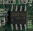 |
An ISSI 4C01-3G , part no IS24C01-3G, a 1 Kbit 400KHz eeprom. Datasheet: http://www.issi.com/pdf/24C01-2.pdf
Probably used to store data such as user settings, last song played and FM presets.
Pins 1, 2 and 3 are used to set the LSBs of the address the 2-wire interface, and are not awfully important to understanding the H1xx. They are tied either to Gnd or Vcc. Pin 4 is Gnd, and pin 8 is Vcc, and these are usually quite obvious due to the thicker PCB traces that lead from them. Vcc should be around 5V and can be easily measured from the lead. Pin 7 is the Write Protect pin and I am sure that it is tied to Gnd, which allows the chip to be writable. If it is tied to Vcc, the chip will be write protected. The final 2 pins are the said 2-wire interface pins. Pin 5 is the Serial DAta (SDA) pin and pin 6 is the Serial CLock (SCL) pin. SCL should be at 400khz, and SDA is the pin used to read or write data.
ISSI IS25C02 - 2kbit EEPROM
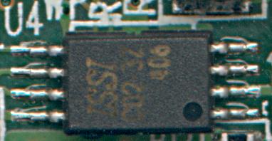 |
An 2 Kbit EEPROM. Datasheet: http://www.issi.com/pdf/25C02.pdf
This is the ISD300 config eeprom is located on the USB/ATA daughterboard.
MEC-AL4A2 - 11.2896MHz oscillator
| |
Side note:
Notice the TA (Transfer Acknowledged) connector right beside MEC-AL4A2.
3.1.10 TA Generation (from http://www.freescale.com/files/dsp/doc/user_guide/M5249C3UM.pdf )
The processor starts a bus cycle by asserting -CSx with the other control signals. The processor then waits for a transfer acknowledgment (-TA) either from within (Auto acknowledge - AA mode) or from the externally addressed device before it can complete the bus cycle. -TA is used to indicate the completion of the bus cycle. It also allows devices with different access times to communicate with the processor properly (i.e. asynchronously) like the Ethernet controller (U4). The MCF5249 processor, as part of the chip-select logic, has a built-in mechanism to generate -TA for all external devices which do not have the capability to generate this signal. For example the Flash ROM cannot generate a -TA.signal. The chip-select logic is programmed by the dBUG ROM Monitor to generate -TA internally after a pre-programmed number of wait states. In order to support future expansion of the M5249C3 board, the -TA input of the processor is also connected to the Processor Expansion Bus (J5, pin 66). This allows any expansion boards to assert this line to provide a -TA signal to the processor. On the expansion boards this signal should be generated through an open collector buffer with no pull-up resistor; a pull-up resistor is included on this board. All -TA signals from expansion boards should be connected to this line.
LVCH16245A - 16-Bit Bus Transceiver With 3-State Outputs
| |
Info: http://focus.ti.com/docs/prod/folders/print/sn74lvch16245a.html
Datasheet: http://www-s.ti.com/sc/ds/sn74lvch16245a.pdf
LW052A - Dual 4-Channel Analog Multiplexer/Demultiplexer
| |
Datasheet: http://rockbox.haxx.se/twiki/pub/Main/IriverInfo/TexasInstrumentsLW052ADataSheet.pdf
This selects between the iriver dac and the internal FM radio for output.
AZU 3AW ZD5L (the 5 could be an S or even an 8)
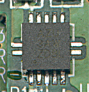 DanHollis: It's pretty clear it's AZU 3AW ZD8L
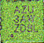
Texas Instruments have now confirmed this to be a BQ24022 Li-Ion charger.
Micropower Synchronous Buck-Boost DC/DC Converter
Markings: LTNP
Maybe the power source for the hard drive?
Datasheet: http://www.linear.com.cn/pdf/3440i.pdf
The LCD module
The LCD module has a few markings on it:
- On the side: 0301W and 3ZA
- On the plastic strip: S4E1 5002
- On the COG chip itself: TF3X23
The LCD connector has 18 pins. Pinout:
| Pin | Function |
|---|---|
| 1 | VCC |
| 2 | GND |
| 3 | D7 |
| 4 | D6 |
| 5 | D5 |
| 6 | D4 |
| 7 | D3 |
| 8 | D2 |
| 9 | D1 |
| 10 | D0 |
| 11 | Unknown (pulled down with 100k to GND) |
| 12 | Maybe CS2 (connected to GND) |
| 13 | OE |
| 14 | R/W |
| 15 | A0 |
| 16 | RESET |
| 17 | CS |
| 18 | GND |
Suggested chip candidates:
- Solomon SSD1854 - The COF (chip-on-flex) drawing in Appendix A is very similar to the Iriver display.
- Epson S1D15E06 (I picked this datasheet in particular because of the following features: 4-level grayscale; adjustable contrast; 160x128 resolution; hardware interface that supports 6800 mpu parallel data interface; minimum pin count required according to Section 11 (2) of the data sheet is 18 PINS: A0, CS1, CS2, RD, WR, RES, VSS, VDD, P/S, C86, and D0 thru D7. -- DaveHooper)
DanHollis: andilcd says it's not one of theirs.
PaulS: Here's a qualifier I think you can use to test whether the display is correct. The commands appear to be sent 8 bits at a time. The initialization sequence looks like a write of the following command bytes: 0xAF, 0xA0, 0xC5, 0xA6, 0xA4, 0xBF, 0xE5. To write pixels to the display, it switches between command mode and data mode by toggling an address line attached to a GPIO: (command) 0xB1 (data) XX (command) 0x13 (data) 0x00 (command) 0x1D (data) XX XX XX ....The Solomon-Systech almost looks reasonable here for the init bytes, with the 0xB1 mapping to "set page address" and 0x13 setting the column. However that's where the suitability ends, since the data write and 0x1D command don't make sense. On the other hand, the Andilcd datasheet matches the commands in a more precise manner, and the 0x1D maps exactly to what you'd expect which is a "data write start" command. So, I'm willing to believe that either a) it's one of these andilcd's and they don't know it or b) it's similar enough that we can use their datasheet to understand what's going on with the display, for the most part.
LinusNielsenFeltzing: The Epson data sheet seems to be it. The current LCD driver is based on it, and it works very well.
The Buttons

On the remote at least, the buttons are attached via a series of resistors in a similar manner to the circuit above. An ADC (see section above) is used to test the voltage at a point within the resistor network. Note that in this configuration, the buttons have an explicit priority order. If switch S1 closes, the state of S2, S3, etc don't matter -- we read back VP * RS / (R0+R1). That is, unless S0 is closed, in which case it wins. The setup I and others probed out of the remote for Rn/Sn pairs is as follows:
| Resistor Value (Ohms) | Switch Name |
| 0 (short) | Stop |
| 270 | Minus (-) |
| 390 | A-B |
| 470 | Plus (+) |
| 680 | Bitrate |
| 820 | Rec |
| 1200 | Source |
| 2700 | Forward (>>) |
| 4700 | Navi |
| 15000 | Back (<<) |
It appears that the internal buttons are attached in a similar manner, attached to a different input on the same ADC.
Remote Control
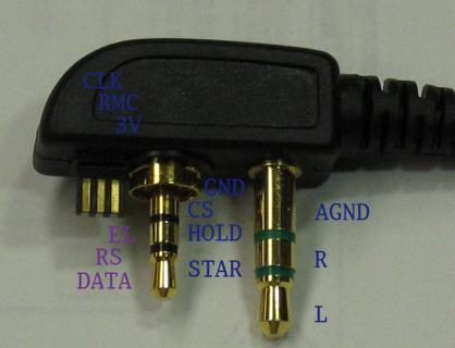
The remote is connected via a composite connector. There are many signals which go back and forth from the unit to the remote. The connections appear to be as follows:
| Pin | Description | Main Connection | Remote Connection |
| AGND | Analog ground for audio | UDA1380TT Codec | Headphone Jack |
| R | Right audio channel | UDA1380TT Codec | Headphone Jack |
| L | Left audio channel | UDA1380TT Codec | Headphone Jack |
| GND | Digital Ground | ||
| CS | LCD display SPI chip select | GPIO34? | LCD Controller |
| HOLD | HOLD switch | GPIO?? | HOLD Switch |
| START | Play button 564 ohm resistor to ground | GPIO37 or 38 | Play Button |
| CLK | LCD display SPI clock | GPIO28? | LCD Controller |
| RMC | Remote control button resistor network | Channel 1 of TLV08341 | 3-way Buttons |
| 3V | Power for the LCD display | ||
| DATA | LCD display SPI data | GPIO50 | LCD Controller |
| RS | "Register Select", switches between control & data registers | GPIO16 | LCD Controller |
| EL | Backlight (I believe I remember this being active-low. -- JacobRosenstein) | GPIO11?? | EL Controller |
LCD Controller - TOMATO TL0324SF8
Datasheet: http://www.rockbox.org/twiki/pub/Main/DataSheets/TL0324S_V02.pdf
The serial interface to the LCD module appears to be wired as write-only, as the WR line doesn't make it out of the remote. The serial communication lines consist of a CLK, DATA, CS (chip select), and RS (register select). 'Register select' toggles whether the serial data is directed into a control register or data register.
Unknown electroluminescent driver chip
JacobRosenstein: I can't tell exactly what chip this is, and I'm not sure it's really necessary to know.
| { Edit | View raw | Attach | Ref-By | Printable | Diffs | r1.52 | > | r1.51 | > | r1.50 | More } |
|
Revision r1.52 - 16 Jun 2005 - 10:47 GMT - HristoKovachev Parents: IriverPort |
Copyright © 1999-2005 by the contributing authors. |
| Main.IriverHardwareComponents moved from Main.HardwareComponents on 12 Sep 2004 - 23:16 by MatthiasWientapper - put it back | |